CXLE8601是一款专为1W LED灯设计的升压恒流驱动器,凭借其0.22V低采样电压和400KHz固定开关频率,提供稳定的输出性能。芯片内置频率补偿电路与功率MOS管,大幅简化外部电路设计,同时支持3~8串LED灵活配置,尤其适用于输入电压≥12V时的高亮度场景。
[ CXLE8601 ]
产品技术资料帮助
查看全部>
一,产品概述(General Description)
CXLE8601是一款专为1W LED灯设计的升压恒流驱动器,凭借其0.22V低采样电压和400KHz固定开关频率,提供稳定的输出性能。芯片内置频率补偿电路与功率MOS管,大幅简化外部电路设计,同时支持3~8串LED灵活配置,尤其适用于输入电压≥12V时的高亮度场景。
The CXLE8602 regulator is fixed frequency PWM Boost (step-up) LED
constant current driver,capable of driving Series 1W LED units with excellent
line and load regulation. The regulator is simple to use because it includes
internal frequency compensation and a fixed-frequency oscillator so that it
requires a minimum number of external components to work.
The CXLE8602 could directly drive 6 Series 1W LED units at VIN>12V .
The CXLE8601 regulator is fixed frequency PWM Boost (step-up) LED
constant current driver,capable of driving Series 1W LED units with excellent
line and load regulation. The regulator is simple to use because it includes
internal frequency compensation and a fixed-frequency oscillator so that it
requires a minimum number of external components to work.
The CXLE8601 could directly drive 5~8 Series 1W LED units at VIN>12V .
The PWM control circuit is able to adjust the duty ratio linearly from 0 to 95%. An enable function, an over current protection function is built inside. An internal compensation block is built in to minimize external component count.
宽压高效驱动
输入电压覆盖3.6V~24V,适配多种电源环境,输入≥12V时可驱动5~8串LED。
92%超高转换效率,搭配最大2A开关电流,确保低能耗、高亮度输出。
精准控制与保护
PWM线性调光:0~90%占空比无级调节,实现平滑亮度调控。
多重防护机制:集成过流保护、热关断、LED开路保护及软启动功能,保障系统安全运行。
高度集成设计
内置补偿模块、电流限制功能及TTL使能控制(EN脚),减少外围元件需求。
SOP8紧凑封装,节省PCB空间,适配小型化设备。
低采样电压:0.22V输出电流检测,提升能效比。
稳定频率输出:400KHz固定频率,降低噪声干扰。
工业级可靠性:支持-40℃~85℃工作温度,适应严苛环境。
二.产品特点(Features)
![]()
Wide 3.6V to 24V Input Voltage Range
0.22V FB adjustable LED drive current
Directly drive 6 Series 1W LED at
VIN>=12V
Fixed 400KHz Switching Frequency
Max. 2A Switching Current Capability
Up to 92% efficiency
Excellent line and load regulation
EN PIN TTL shutdown capability
Internal Optimize Power MOSFET
Built in Soft-Start Function
Built in Frequency Compensation
Built in Thermal Shutdown Function
Built in Current Limit Function
Available in SOP8L package
三,应用范围 (Applications)![]()
LED照明系统:通用照明、景观灯、工业灯具。
显示设备背光:7~15寸LCD面板、显示器LED背光驱动。
便携设备:电池供电场景下的高效升压恒流解决方案。
CXLE8601以高集成度、低功耗和卓越稳定性,成为LED驱动领域的优选方案,广泛适用于消费电子、工业控制及显示技术领域。
LED Lighting
Boost constant current driver
Monitor LED Backlighting
7’ to 15’ LCD Panels
四.技术规格书下载(产品PDF)![]()
需要详细的PDF规格书请扫一扫微信联系我们,还可以获得免费样品以及技术支持!

五,产品封装图 (Package)![]()

|
Pin Number |
Pin Name |
Description |
|
1 |
EN |
Enable Pin. Drive EN pin low to turn off the device, drive it |
|
2 |
VIN |
Supply Voltage Input Pin. CXLE8602 operates from a 3.6V to 24V |
|
3 |
FB |
Feedback Pin (FB). The feedback threshold voltage is 0.22V. |
|
4 |
NC |
No Connected. |
|
5,6 |
SW |
Power Switch Output Pin (SW). Output is the switch node that |
|
7,8 |
GND |
Ground Pin. |
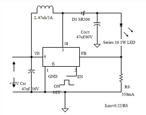
六.电路原理图![]()
七,功能概述![]()
|
Parameter |
Symbol |
Value |
Unit |
|
Input Voltage |
Vin |
-0.3 to 26 |
V |
|
Feedback Pin Voltage |
VFB |
-0.3 to Vin |
V |
|
EN Pin Voltage |
VEN |
-0.3 to Vin |
V |
|
Output Switch Pin Voltage |
VOutput |
-0.3 to 60 |
V |
|
Power Dissipation |
PD |
Internally limited |
mW |
|
Thermal Resistance (SOP8) |
RJA |
100 |
oC/W |
|
Operating Junction Temperature |
TJ |
-40 to 125 |
oC |
|
Storage Temperature |
TSTG |
-65 to 150 |
oC |
|
Lead Temperature (Soldering, 10 sec) |
TLEAD |
260 |
oC |
|
ESD (HBM) |
>2000 |
V |
八,相关芯片选择指南![]()
| 产品型号 | 输入电压 | 最大输出电压 | 开关电流 | 开关频率 | 恒流设置 | 封装形式 |
| CXLE8601 | 3.6V ~ 24V | 32V | 2A | 400KHz | Adj (0.22V) | SOP8L |
| CXLE8602 | 5V ~ 40V | 60V | 2A | 400KHz | Adj (0.22V) | SOP8L |
| CXLE8603 | 5V ~ 40V | 60V | 2A | 400KHz | Adj (0.22V) | SOP8L |
| CXLE8604 | 3.6V ~ 32V | 60V | 4A | 180KHz | Adj (0.22V) | TO252-5L |
| CXLE8605 | 5V ~ 32V | 60V | 5A | 180KHz | Adj (0.22V) | TO263-5L |
九。Bill of Materials(BOM)
十。Performance Data

十一.Populated Circuit Board Photograph

十二.PCB Layout

Note:
1. Keep feedback wiring away from inductor and schottky.
2. VIN, SW, LED+, LED- lines must be short and ground plane construction for best results.
3. C3,R1,R2 and R3 are used for the designing with PWM dimming. If not with PWM dimming, R1 replaced
with 0 ohm, C3,R2,R3 open.