CXSD62136B采用电流模式控制方案设计,可以将4.5V到24V的宽输入电压转换为0.92V到20V的可调输出电压,提供良好的输出电压调节
[ 产品资料下载 ]
产品技术资料帮助
查看全部>
1.产品概述 2.产品特点
3.应用范围 4.下载产品资料PDF文档
5.产品封装图 6.电路原理图
7.功能概述 8.相关产品
一,产品概述(General Description) CXSD62136 CXSD62136B is a 2A synchronous buck converter with integrated power MOSFETs.The CXSD62136 CXSD62136B design with a current-mode control scheme, can convert wide input voltage of 4.5V to 24V to the output voltage adjustable from 0.92V to 20V to provide excellent output voltage regulation. The CXSD62136 CXSD62136B is also equipped with Power-on-reset, softstart, and whole protections (over-temperature, and current-limit) into a single package.This device, available SOP-8, provides a very compact system solution external components and PCB area
二.产品特点(Features)
Wide Input Voltage from 4.5V to 24V
2A Continuous Output Current
Adjustable Output Voltage from 0.92V to 20V
Intergrated N-MOSFET
Fixed 340kHz Switching Frequency
Stable with Low ESR Capacitors
Power-On-Reset Detection
Programmable Soft-Start
Over-Temperature Protection
Over-Voltage Protection
Current-Limit Protection with Frequency Foldback
Enable/Shutdown Function
Small SOP-8 Package
Lead Free and Green Devices Available (RoHS Compliant)
三,应用范围 (Applications)
LCD Monitor/TV
Set-Top Box
DSL, Switch HUB
Notebook Computer
四.下载产品资料PDF文档
需要详细的PDF规格书请扫一扫微信联系我们,还可以获得免费样品以及技术支持!

五,产品封装图 (Package)

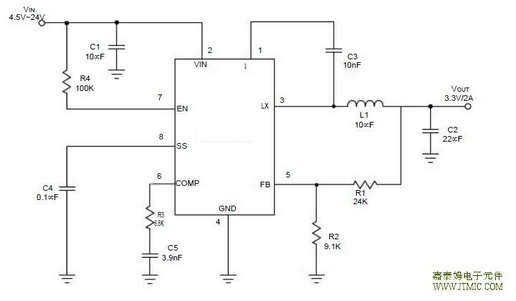
六.电路原理图
七,功能概述
Main Control Loop The CXSD62136 CXSD62136B is a constant frequency current mode switching regulator. During normal operation, the inter-
nal N-channel power MOSFET is turned on each cycle when the oscillator sets an internal RS latch and would
be turned off when an internal current comparator (ICMP) resets the latch. The peak inductor current at which ICMP
resets the RS latch is controlled by the voltage on the COMP pin, which is the output of the error amplifier
(EAMP). An external resistive divider connected between VOUT and ground allows the EAMP to receive an output
feedback voltage VFB at FB pin. When the load current increases, it causes a slight decrease in VFB relative to
the 0.92V reference, which in turn causes the COMP volt- age to increase until the average inductor current matches
the new load current.
VIN Power-On-Reset (POR) and EN Under-voltage Lockout
The CXSD62136 CXSD62136B keep monitoring the voltage on VIN pin to prevent wrong logic operations which may occur when VIN voltage is not high enough for the internal control circuitry to operate. The VIN POR has a rising threshold
of 4.1V (typical) with 0.5V of hysteresis.An external under-voltage lockout (UVLO) is sensed at the EN pin. The
EN UVLO has a rising threshold of 2.5V with 0.2V of hysteresis. The EN pin should be connected
a resistor divider from VIN to EN.After the VIN and EN voltages exceed their respective voltage thresholds,
the IC starts a start-up process and then ramps up the output voltage to the setting of output voltage.
Over-Temperature Protection (OTP)
The over-temperature circuit limits the junction tempera-ture of the CXSD62136 CXSD62136B. When the junction temperature ex-ceeds TJ = +160oC, a thermal sensor turns off the power MOSFET, allowing the devices to cool. The thermal sen-sor allows the converter to start a start-up process and regulate the output voltage again after the junction tem-
perature cools by 50oC.The OTP is designed with a 50oC hysteresis to lower the average TJ during continuous thermal overload conditions,increasing lifetime of the lC.
Enable / Shutdown
Driving EN to ground places the CXSD62136 CXSD62136B in shutdown. When in shutdown, the internal power MOSFET turns off,all internal circuitry shuts down.
Current-Limit Protection
The CXSD62136 CXSD62136B monitors the output current, flowing through the N-Channel power MOSFET, and limits the
IC from damages during overload, short-circuit and over- voltage conditions.
Frequency Foldback
The foldback frequency is controlled by the FB voltage.When the FB pin voltage is under 0.6V, the frequency of
the oscillator will be reduced to 110kHz. This lower fre-quency allows the inductor current to safely discharge,
thereby preventing current runaway. The oscillator’s fre-quency will switch to its designed rate when the feedback
voltage on FB rises above the rising frequency foldback threshold (0.6V, typical) again.
Over-Voltage Protection
The over-voltage function monitors the output voltage by FB pin. When the FB voltage increase over 120% of the
reference voltage, the over-voltage protection compara-tor will force the low-side MOSFET gate driver high. This
action actively pulls down the output voltage. As soon as the output voltage is within regulation, the OVP compara-
tor is disengaged. The chip will restore its normal operation.
八,相关产品 更多同类产品.......
|
Switching Regulator > Buck Converter |
|||||||||||
|
Part_No |
Package |
Architectu |
No.of PWM Outpu |
Drive Lout (A) |
Vin(V) |
Fmax Khz |
Vref (V) |
R-Top (milohm) |
R-Sync (milohm) |
Iq (No load) (uA) |
|
|
min |
max |
||||||||||
|
TQFN5x6-28 |
CM |
1 |
5 |
4.5 |
26 |
380 |
0.8 |
50 |
20 |
1000 |
|
|
SOP-8 |
CM |
1 |
2 |
4.5 |
26 |
380 |
0.8 |
100 |
1000 |
||
|
SOP-8P |
CM |
1 |
4 |
4.5 |
26 |
380 |
0.8 |
80 |
1000 |
||
|
SOT23-5|TSOT23-5 |
CM |
1 |
1 |
2.7 |
6 |
1500 |
0.6 |
280 |
250 |
25 |
|
|
SOT23-5 |
CM |
1 |
1 |
2.7 |
6 |
1500 |
0.6 |
280 |
250 |
||
|
SOP-8 |
CM |
1 |
3 |
4.3 |
14 |
500 |
0.8 |
70 |
70 |
500 |
|
|
SOP-8P |
CM |
1 |
3 |
4.3 |
14 |
500 |
0.8 |
55 |
45 |
500 |
|
|
TDFN3x3-10 |
3 |
2.6 |
5.5 |
2000 |
0.8 |
110 |
110 |
460 |
|||
|
TDFN3x3-10 |
CM |
2 |
1 |
2.7 |
6 |
1500 |
0.6 |
280 |
250 |
500 |
|
|
TDFN3x3-10 |
CM |
2 |
1 |
2.7 |
6 |
1500 |
0.6 |
280 |
250 |
||
|
TDFN2x2-6 |
CM |
1 |
1 |
2.7 |
6 |
1500 |
0.6 |
280 |
250 |
25 |
|
|
TDFN2x2-6 |
CM |
1 |
1 |
2.7 |
6 |
1500 |
0.6 |
280 |
250 |
||
|
TDFN3x3-12 |
CM |
2 |
1 |
2.7 |
6 |
1500 |
0.6 |
280 |
250 |
25 |
|
|
TDFN3x3-12 |
CM |
2 |
1 |
2.7 |
6 |
1500 |
0.6 |
280 |
250 |
||
|
TDFN 3x3 12 |
CM |
2 |
1 |
3 |
5.5 |
1500 |
0.6 |
280 |
250 |
30 |
|
|
TQFN3x3-20 |
CM |
3 |
2 |
2.9 |
5.5 |
1500 |
0.6 |
- |
- |
300 |
|
|
TDFN2x2-8 |
CM |
1 |
1 |
3.3 |
8 |
1500 |
0.6 |
280 |
250 |
25 |
|
|
SOP-8 |
CM |
1 |
2 |
4.5 |
24 |
340 |
0.925 |
110 |
110 |
1900 |
|
|
SOP-8P |
CM |
1 |
3 |
4.5 |
24 |
340 |
0.925 |
110 |
110 |
1900 |
|
|
SOP-8 |
CM |
1 |
2 |
4.5 |
24 |
340 |
0.92 |
130 |
130 |
1900 |
|
|
SOP-8P |
CM |
1 |
2 |
4.5 |
24 |
340 |
0.92 |
130 |
130 |
1900 |
|
|
SOP-8P |
CM |
1 |
3 |
4.5 |
24 |
340 |
0.92 |
85 |
85 |
1900 |
|
|
SOP-8P |
CM |
1 |
4 |
4.5 |
24 |
340 |
0.8 |
85 |
85 |
1900 |
|
|
TSOT-23-8A |
CM |
1 |
3 |
4.5 |
24 |
500 |
0.807 |
100 |
40 |
1000 |
|
|
TSOT-23-8A |
CM |
1 |
3 |
4.5 |
24 |
500 |
0.807 |
100 |
40 |
1000 |
|
|
TSOT-23-8A |
CM |
1 |
2 |
4.5 |
24 |
500 |
0.807 |
115 |
50 |
1000 |
|
|
SOP-8P |
CM |
1 |
3 |
4.5 |
24 |
1300 |
0.925 |
110 |
110 |
1900 |
|
|
SOP-8 |
CM |
1 |
2 |
4.5 |
24 |
340 |
0.925 |
110 |
110 |
1900 |
|
|
SOP-8P |
CM |
1 |
3 |
4.5 |
24 |
340 |
0.925 |
110 |
110 |
1900 |
|
|
TSOT-23-8A |
CM |
1 |
2 |
4.5 |
24 |
500 |
0.807 |
115 |
50 |
500 |
|
|
TSOT-23-8A |
CM |
1 |
3 |
4.5 |
24 |
500 |
0.807 |
100 |
40 |
500 |
|
|
TSOT-23-6 |
COT |
1 |
2 |
4.6 |
16 |
500 |
0.6 |
110 |
100 |
50 |
|
|
TSOT-23-6 |
COT |
1 |
2 |
4.6 |
16 |
500 |
0.8 |
95 |
40 |
50 |
|
|
TSOT-23-6 |
COT |
1 |
3 |
4.6 |
16 |
500 |
0.8 |
90 |
35 |
50 |
|
|
TSOT-23-8A |
CM |
1 |
2.5 |
4.5 |
24 |
500 |
0.807 |
140 |
60 |
1000 |
|
|
TSOT-23-6,TDFN2x2-6 |
COT |
1 |
3 |
4.6 |
16 |
500 |
0.6 |
110 |
80 |
50 |
|
|
SOP8P|TDFN3x3-10 |
CM |
1 |
2 |
2.5 |
6 |
1000 |
0.8 |
85 |
75 |
460 |
|
|
SOP8P|TDFN3x3-10 |
CM |
1 |
3.2 |
2.5 |
6 |
1000 |
0.8 |
85 |
75 |
460 |
|
|
SOP8P|TDFN3x3-10 |
CM |
1 |
4 |
2.5 |
6 |
500 |
0.8 |
85 |
75 |
460 |
|
|
SOP-8P |
CM |
1 |
5 |
2.5 |
6 |
1000 |
0.6 |
65 |
55 |
460 |
|
|
TDFN 2x2 12 |
CM |
1 |
3.5 |
2.7 |
5.5 |
1320 |
0.6 |
70 |
60 |
40 |
|
|
SOP-8 |
CM |
1 |
2 |
4.5 |
24 |
340 |
0.8 |
110 |
110 |
1900 |
|
|
SOP-8P |
CM |
1 |
3 |
4.5 |
24 |
340 |
0.8 |
110 |
110 |
1900 |
|
|
TDFN3x3-10 |
CM |
1 |
2 |
4.5 |
24 |
340 |
0.8 |
110 |
110 |
1900 |
|
|
TDFN3x3-10 |
CM |
1 |
3 |
4.5 |
24 |
340 |
0.8 |
110 |
110 |
1900 |
|
|
TSOT-23-8A |
CM |
1 |
2 |
4.5 |
24 |
500 |
0.791 |
115 |
50 |
1000 |
|
|
TSOT-23-8A |
CM |
1 |
3 |
4.5 |
24 |
500 |
0.791 |
100 |
40 |
1000 |
|
|
TSOT-23-8A |
CM |
1 |
3 |
7 |
24 |
500 |
0.791 |
100 |
40 |
1000 |
|
|
TDFN 2x2-6 |
CM |
1 |
1 |
3 |
5.5 |
1500 |
0.6 |
260 |
230 |
30 |
|
|
SOT23-5,TSOT23-5A |
CM |
1 |
1.2 |
3 |
5.5 |
1500 |
0.6 |
260 |
230 |
30 |
|
|
SOT23-5,TSOT23-5A |
CM |
1 |
1 |
3 |
5.5 |
1500 |
0.6 |
260 |
230 |
30 |
|
|
SOT23-5,TSOT23-5A |
CM |
1 |
1 |
3 |
5.5 |
1500 |
0.6 |
260 |
230 |
30 |
|
|
SOT23-5,TSOT23-5A |
CM |
1 |
1.2 |
3 |
5.5 |
1500 |
0.6 |
260 |
230 |
30 |
|
|
SOT23-5,TSOT23-5A |
CM |
1 |
1 |
3 |
5.5 |
1500 |
0.6 |
260 |
230 |
30 |
|
|
TSOT-23-8A |
CM |
1 |
2 |
4.5 |
24 |
800 |
0.807 |
115 |
50 |
1000 |
|
|
TSOT-23-8A |
CM |
1 |
3 |
4.5 |
24 |
800 |
0.807 |
100 |
40 |
1000 |
|
|
TSOT-23-8A |
CM |
1 |
2 |
4.5 |
24 |
500 |
0.807 |
115 |
50 |
1000 |
|
|
TDFN5x5-16 |
CM |
1 |
4 |
4.5 |
26 |
380 |
0.8 |
22 |
- |
1000 |
|
|
TDFN 2x2-8 |
CM |
1 |
0.8 |
4.5 |
5.5 |
1700 ~ 2300 |
0.6 |
300 |
|||
|
TQFN 4x4 22 |
COT |
1 |
8 |
2.7 |
28 |
100~1000 |
0.8 |
30 |
9 |
700 |
|
|
TQFN4x4-23 |
COT |
1 |
6 |
2.7 |
28 |
100~1000 |
0.8 |
30 |
9 |
750 |
|
|
TQFN 4x4 23 |
COT |
1 |
8 |
2.7 |
28 |
100~1000 |
0.8 |
30 |
9 |
700 |
|
|
TQFN 4x4 23 |
COT |
1 |
8 |
2.7 |
28 |
100~1000 |
0.8 |
30 |
9 |
700 |
|
|
TQFN 4x4 23 |
COT |
1 |
10 |
2.7 |
28 |
100~1000 |
0.8 |
27 |
7 |
700 |
|
|
TQFN 4x4 23 |
COT |
1 |
10 |
2.7 |
28 |
100~1000 |
0.8 |
27 |
7 |
700 |
|
|
TQFN 4x4 23 |
COT |
1 |
10 |
2.7 |
28 |
100~1000 |
0.8 |
27 |
7 |
700 |
|
|
TQFN 4x4 23 |
COT |
1 |
10 |
2.7 |
28 |
100~1000 |
0.8 |
27 |
7 |
700 |
|
|
TQFN 4x4 23 |
COT |
1 |
8 |
2.7 |
28 |
100~1000 |
0.8 |
30 |
9 |
25 |
|
|
TQFN 4x4 23 |
COT |
1 |
6 |
2.7 |
28 |
100~1000 |
0.8 |
30 |
12 |
700 |
|
|
TQFN 4x4 23 |
COT |
1 |
6 |
2.7 |
28 |
100~1000 |
0.8 |
30 |
12 |
700 |
|
|
TQFN 4x4 23 |
COT |
1 |
6 |
2.7 |
28 |
100~1000 |
0.8 |
30 |
12 |
700 |
|
|
TQFN 4x4 23 |
COT |
1 |
6 |
2.7 |
28 |
100~1000 |
0.8 |
30 |
12 |
700 |
|
|
TQFN 4x4 23 |
COT |
1 |
8 |
2.7 |
28 |
100~1000 |
0.8 |
30 |
12 |
25 |
|
|
TQFN5x5 30 |
COT |
1 |
12 |
2.7 |
28 |
300~1000 |
0.8 |
9.7 |
5.2 |
700 |
|
|
TQFN5x5 30 |
COT |
1 |
12 |
2.7 |
28 |
300~1000 |
0.8 |
14.6 |
7.8 |
750 |
|
|
TQFN5x6-28 |
COT |
1 |
8 |
3 |
25 |
500 |
0.75 |
12 |
12 |
400 |
|
|
TDFN3x3-10 |
CM |
1 |
3 |
2.6 |
6 |
1000 |
0.6 |
65 |
55 |
460 |
|
|
TDFN3x3-10 |
CM |
1 |
3 |
2.6 |
5.5 |
1000 |
0.6 |
65 |
55 |
65 |
|
|
TDFN3x3-10 |
CM |
1 |
3 |
2.6 |
6 |
1000 |
0.6 |
75 |
55 |
460 |
|
|
TDFN3x3 10 |
CM |
1 |
3 |
2.6 |
6 |
1000 |
0.8 |
75 |
55 |
460 |
|
|
TDFN3x3 10 |
CM |
1 |
3 |
2.6 |
6 |
1000 |
0.8 |
75 |
55 |
460 |
|
|
TQFN3x3-16 |
COT |
1 |
8 |
6 |
28 |
500 |
0.6 |
24 |
14 |
80 |
|
|
TSOT23-6 |
CM |
1 |
1 |
2.7 |
5.5 |
1500 |
0.6 |
280 |
250 |
25 |
|
|
SOT23-6, TDFN2x2 8 |
CM |
1 |
3 |
2.6 |
6 |
1000 |
0.6 |
110 |
80 |
50 |
|
|
TDFN3x3-10 |
CM |
1 |
3 |
4.5 |
24 |
600 |
0.8 |
70 |
70 |
400 |
|
|
TQNF4x4 32 |
COT |
1 |
8 |
4.5 |
26 |
400~550 |
0.75 |
75 |
75 |
230 |
|
|
TQN 4x4 26 |
COT |
2 |
8 |
4.5 |
25 |
400~1400 (VDDQ) 1000(VPP) |
0.6V for VPPSMBUS for VDDQ=1.0V~1.2V |
20(VDDQ) 200(VPP) |
7(VDDQ) 200(VPP) |
270 |
|
◀ 上一篇:CXSD62136功率mosfet 2A连续输出电流同步buck变换器4.5V宽输入电压转换为24V固定340kHz开关频率低ESR电容稳定
下一篇▶:340kHz同步降压转换器CXSD62137 功率mosfet的3A同步降压转换器采用电流模式控制方案