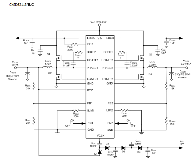
CXSD62113E线性稳压器为备用电源提供5V和3.3V输出。线性调节器提供高达100毫安的输出电流。当PWMx输出电压高于LDOx旁路阈值时,相关LDOx稳压器关闭,其输出通过内部切换MOSFET连接到VOUTx。它可以节省功耗。电荷泵电路采用70kHz时钟驱动器,使用VUT1作为其电源,以产生接近15V直流电压的AP。
[ 产品资料下载 ]
产品技术资料帮助
查看全部>
目录
1.产品概述 2.产品特点
3.应用范围 4.下载产品资料PDF文档
5.产品封装图 6.电路原理图
7.功能概述 8.相关产品
一,产品概述(General Description)
The CXSD62113 CXSD62113A CXSD62113B CXSD62113C CXSD62113E integrates dual step-down, constant-on-time,synchronous PWM controllers (that drives dual N-channel MOSFETs for each channel) and two low drop-out regulators as well as various protections into a chip.The PWM controllers step down high voltage of a battery to generate low-voltage for NB applications. The output of PWM1 and PWM2 can be adjusted from 2V to 5.5V by setting a resistive voltage-divider from VOUTx to GND.
The linear regulators provide 5V and 3.3V output for standby power supply. The linear regulators provide up to 100mA output current. When the PWMx output voltage is higher than LDOx bypass threshold, the related LDOx regulator is shut off and its output is connected to VOUTx by internal switchover MOSFET. It can save power dissipation. The charge pump circuit with 270kHz clock driver uses VOUT1 as its power supply to generate ap-proximately 15V DC voltage.
The CXSD62113/A/B/C provides excellent transient response and accurate DC output voltage in either PFM or PWM Mode. In Pulse-Frequency Mode (PFM), the
CXSD62113/A/B/C provides very high efficiency over light to heavy loads with loading-modulated switching frequencies. The Forced-PWM Mode works nearly at
constant frequency for low-noise requirements. The unique ultrasonic mode maintains the switching frequency above 25kHz, which eliminates noise in
audio application.
The CXSD62113/A/B/C is equipped with accurate sourc-ing and current-limit, output under-voltage output over-voltage protections, being perfect for NB applications. A 1.4ms (typ.) digital soft-start can reduce the start-up current. A soft-stop function actively discharges the output capacitors by the discharge device. The CXSD62113/A/B has individual enable controls for each PWM channels. Pulling both EN1/2 pin low shuts down the all of outputs unless LDO3 output. The LDO3 and LDO5 of CXSD62113A/C are always on standby power.
The CXSD62113/A/B/C is available in a TQFN3x3-20 package.
二.产品特点(Features)
Wide Input voltage Range from 6V to 25V
Provide 5 Independent Outputs with ±1.0% Accuracy Over-Temperature
- PWM1 Controller with Adjustable (2V to 5.5V) Out-put
PWM2 Controller with Adjustable (2V to 5.5V) Out-put
100mA Low Dropout Regulator (LDO5) with Fixed 5V Output
100mA Low Dropout Regulator (LDO3) with Fixed 3.3V Output
270kHz Clock Signal for 15V Charge Pump (Used VOUT1 as Its Power Supply)
Excellent Line/Load Regulations about ±1.5% Over-Temperature Range
Built in POR Control Scheme Implemented
Constant On-Time Control Scheme with Frequency
Compensation for PWM Mode
Selectable Switching Frequency in PWM Mode
Built-in Digital Soft-Start for PWM Outputs and Soft-
Stop for PWM Outputs and LDO Outputs
Integrated Bootstrap Forward P-CH MOSFET
High Efficiency over Light to Full Load Range (PWMs)
Built-in Power Good Indicators (PWMs)
Independent Enable Inputs (PWMs, LDO)
70% Under-Voltage and 125% Over-Voltage Protec-tions (PWM)
Adjustable Current-Limit Protection (PWMs)
- Using Sense Low-Side MOSFET’s RDS(ON)
Over-Temperature Protection
3mmx3mm Thin QFN-20 (TQFN3x3-20) package
Lead Free and Green Device Available (RoHS Compliant)
三,应用范围 (Applications)
Notebook and Sub-Notebook Computers
Portable Devices
DDR1, DDR2, and DDR3 Power Supplies
3-Cell and 4-Cell Li+ Battery-Powered Devices
Graphic Cards
Game Consoles
Telecommunications
四.下载产品资料PDF文档
需要详细的PDF规格书请扫一扫微信联系我们,还可以获得免费样品以及技术支持!

五,产品封装图 (Package)


六.电路原理图

七,功能概述
|
Switching Regulator > Buck Controller |
||||||||||
|
Part_No |
Package |
Archi tectu |
Phase |
No.of PWM Output |
Output Current (A) |
Input Voltage (V) |
Reference Voltage (V) |
Bias Voltage (V) |
Quiescent Current (uA) |
|
|
min |
max |
|||||||||
|
SOP-14 QSOP-16 QFN4x4-16 |
VM |
1 |
1 |
30 |
2.9 |
13.2 |
0.9 |
12 |
8000 |
|
|
SOP-8 |
VM |
1 |
1 |
20 |
2.9 |
13.2 |
0.8 |
12 |
5000 |
|
|
SOP-8 |
VM |
1 |
1 |
20 |
2.9 |
13.2 |
0.8 |
12 |
5000 |
|
|
QFN4x4-24 |
VM |
2 |
1 |
60 |
3.1 |
13.2 |
0.6 |
12 |
5000 |
|
|
SOP-8 |
VM |
1 |
1 |
20 |
2.2 |
13.2 |
0.8 |
5~12 |
2100 |
|
|
SOP-8 |
VM |
1 |
1 |
20 |
2.2 |
13.2 |
0.8 |
5~12 |
2100 |
|
|
SOP8|TSSOP8 |
VM |
1 |
1 |
5 |
5 |
13.2 |
1.25|0.8 |
5~12 |
3000 |
|
|
SOP-8 |
VM |
1 |
1 |
10 |
3.3 |
5.5 |
0.8 |
5 |
2100 |
|
|
SOP-14 |
VM |
1 |
1 |
10 |
5 |
13.2 |
0.8 |
12 |
2000 |
|
|
TSSOP-24 |QFN5x5-32 |
VM |
1 |
2 |
20 |
5 |
13.2 |
0.6 |
5~12 |
4000 |
|
|
SOP14 QSOP16 QFN-16 |
VM |
1 |
1 |
30 |
2.9 |
13.2 |
0.9 |
12 |
4000 |
|
|
SOP-14 |
VM |
1 |
1 |
30 |
2.2 |
13.2 |
0.6 |
12 |
5000 |
|
|
SOP-14 |
VM |
1 |
1 |
30 |
2.2 |
13.2 |
0.6 |
12 |
5000 |
|
|
SOP-14 |
VM |
1 |
1 |
25 |
2.2 |
13.2 |
0.8 |
12 |
5000 |
|
|
LQFP7x7 48 TQFN7x7-48 |
VM |
1 |
6 |
0.015 |
1.4 |
6.5 |
- |
5 |
1800 |
|
|
TSSOP-24P |
VM |
1 |
2 |
20 |
2.97 |
5.5 |
0.8 |
5~12 |
5000 |
|
|
SOP-14 |
VM |
1 |
1 |
10 |
5 |
13.2 |
0.8 |
12 |
3000 |
|
|
SOP-8-P|DIP-8 |
VM |
1 |
1 |
30 |
2.9 |
13.2 |
1.2 |
12 |
3000 |
|
|
SSOP28 QFN4x4-24 |
VM |
1 |
2 |
20 |
5 |
24 |
0.9 |
5 |
1200 |
|
|
SOP-20 |
VM |
1 |
2 |
20 |
2.2 |
13.2 |
0.6 |
5~12 |
4000 |
|
|
SOP8|DFN3x3-10 |
VM |
1 |
2 |
- |
- |
- |
- |
5~12 |
550 |
|
|
DIP8|SOP-8 |
VM |
1 |
1 |
1 |
1.2 |
9 |
24 |
5 |
9 ~ 24 |
|
|
SSOP16 QFN4x4-16 TQFN3x3-16 |
VM |
1 |
1 |
25 |
3 |
25 |
0.6 |
5 |
1700 |
|
|
TDFN3x3-10 |
COT |
1 |
1 |
25 |
3 |
25 |
0.5 |
5 |
350 |
|
|
QFN4x4-24 |
CM |
2 |
1 |
40 |
4.5 |
13.2 |
0.6 |
5~12 |
4000 |
|
|
SOP8P TDFN3x3-10 |
VM |
1 |
1 |
20 |
3 |
13.2 |
0.8 |
5~12 |
2500 |
|
|
SOP8P |
VM |
1 |
1 |
25 |
3 |
13.2 |
0.6|0.8 |
5~12 |
1200 |
|
|
TDFN3x3-10 |
VM |
1 |
1 |
25 |
4 |
13.2 |
0.8 |
5~12 |
2000 |
|
|
TDFN3x3-10 |
COT |
1 |
1 |
25 |
4.5 |
25 |
0.6 |
5~12 |
80 |
|
|
SOP-8P |
VM |
1 |
1 |
25 |
4.5 |
13.2 |
0.8 |
5~12 |
16000 |
|
|
TQFN3x3-10 |
VM |
1 |
1 |
25 |
4.5 |
13.2 |
0.6 |
5~12 |
2500 |
|
|
TDFN3x3-10 |
COT |
1 |
1 |
30 |
3 |
25 |
0.8 |
5~12 |
2000 |
|
|
TQFN3x3-16 |
COT |
1 |
1 |
30 |
1.8 |
28 |
0.6 |
5 |
600 |
|
|
TQFN 3x3 16 |
COT |
1 |
1 |
30 |
1.8 |
28 |
0.6 |
5 |
600 |
|
|
QFN4x4-24 |
VM |
2 |
1 |
50 |
4.5 |
13.2 |
0.6 |
5~12 |
5000 |
|
|
TQFN4x4-24 |
COT |
1 |
2 |
15 |
6 |
25 |
2 |
N |
550 |
|
|
TQFN4x4-24 |
COT |
1 |
2 |
15 |
6 |
25 |
2 |
N |
550 |
|
|
TQFN4x4-4 TQFN3x3-20 |
COT |
1 |
2 |
20 |
3 |
28 |
0.75 |
5 |
800 |
|
|
TQFN3x3-16 |
COT |
1 |
1 |
20 |
1.8 |
28 |
0.75 |
5 |
400 |
|
|
QFN3.5x3.5-14 TQFN3x3-16 |
COT |
1 |
1 |
20 |
1.8 |
28 |
0.75 |
5 |
400 |
|
|
TQFN3x3-16 |
COT |
1 |
2 |
20 |
1.8 |
28 |
0.75 |
5 |
400 |
|
|
QFN3x3-20 TQFN3x3-16 |
COT |
1 |
2 |
20 |
3 |
28 |
1.8|1.5|0.5 |
5 |
740 |
|
|
TQFN4x4-24 |QFN3x3-20 |
CM |
1 |
2 |
15 |
5 |
28 |
0.5 |
N |
3000 |
|
|
TDFN3x3-10 |
COT |
1 |
1 |
20 |
1.8 |
28 |
0.5 |
5 |
250 |
|
|
TQFN3x3-20 |
COT |
1 |
2 |
15 |
6 |
25 |
2 |
N |
550 |
|
|
TQFN 3x3 20 |
COT |
2 |
2 |
11 |
6 |
25 |
2 |
N |
550 |
|
|
TQFN3x3-20 |
COT |
2 |
2 |
11 |
5.5 |
25 |
2 |
N |
280 |
|
|
QFN4x4-24 |
VM |
2 |
1 |
60 |
3.1 |
13.2 |
0.85 |
12 |
5000 |
|
|
SOP-8P |
VM |
1 |
1 |
20 |
2.9 |
13.2 |
0.8 |
12 |
16000 |
|
|
SOP-20 |
VM |
2 |
2 |
30 |
10 |
13.2 |
1 |
12 |
5000 |
|
|
TDFN3x3-10 |
COT |
1 |
1 |
25 |
1.8 |
28 |
0.7 |
5 |
250 |
|
|
TQFN3x3-20 |
COT |
2 |
1 |
40 |
1.8 |
25 |
REFIN Setting |
5 |
700 |
|
|
QFN 3x3 20 TQFN 3x3 16 |
COT |
1 |
2 |
20 |
3 |
28 |
1.8|1.5 1.35|1.2 0.5 |
5 |
800 |
|
|
TQFN3x3 20 |
COT |
1 |
2 |
15 |
3 |
28 |
0.75 |
5 |
220 |
|
|
TQFN3x3 20 |
COT |
1 |
2 |
15 |
3 |
28 |
0.75 |
5 |
220 |
|
|
TQFN3x3-20 |
COT |
1 |
2 |
20 |
3 |
28 |
0.75 |
5 |
180 |
|
◀ 上一篇:CXSD62113|C双降压恒定开启时间同步的PWM控制器每个通道驱动双N通道mosfet
下一篇▶:两个低电压降调节器CXSD62114双降压恒定时间同步PWM控制器内部转换MOSFET