CXUS7718 CXUS7719的程序内存大小大于2K,但CALL和GOTO指令的地址范围只有11位。这个11位地址范围允许一个2K程序内存页大小的分支。为了允许CALL和GOTO指令寻址CX8PU86LV CXUS7719的整个6K程序内存地址范围,还有两个位用于指定程序内存页。分页位来自ROMBANK[1:0]位(PUMODE[6:5])。在执行调用或转到指令时,用户必须确保页面位ROMBANK[1:0]已编程,以便寻址所需的程序内存页面。当其中一条返回指令被执行时,整个13位PC将从堆栈中弹出。因此,返回指令不需要操纵ROMBANK[1:0]
符合USB规范
支持全速和低速USB 2.0规范。
内置USB收发器。
内置1.5k拉高电阻。
支持一个地址和四个8字节和两个32字节的数据终结点。
支持USB暂停和恢复功能。
一个控件输入/输出端点,两个INT,大容量端点。
8位RISC微处理器
6K x 14内部程序OTP-ROM。
256字节内部SRAM。
可选12MHz/24MHz内部MCU时钟(按配置)。
可选默认值/16MHz/12MHz/6MHz/58KHz固件内部MCU时钟。
一个看门狗定时器,定时器0,定时器1,和两个捕获定时器。
系统时钟
内部振荡器
内部正负4%24MHz振荡器
接收到USB流量后,准确率为0.25%。
内部慢振荡器58KHz自由运行时钟暂停模式。
内置可灵活编程的外部振荡器或晶体锁相环
振荡器/晶体的工作频率范围为2~48mhz。
可选外部陶瓷谐振器或内部时钟模式..16-II/O端口
任何GPIO引脚上的高电流驱动器:25毫安/引脚电流接收器。
每个GPIO引脚支持高阻抗输入、内部上拉,
开漏输出,或CMOS输出。
电源管理和消耗
上电复位(POR)为2.0V
芯片可以在2.2V以上的电源下工作。
低电压检测为3.8V
调节器3.3V输出,提供45mA电流。
在24MHz时钟下工作的MCU
启用USB工作电流为17毫安,因为Vcc=5伏。
禁用USB操作电流为6毫安,因为Vcc=3.3伏。
以12MHz时钟运行的MCU
启用USB工作电流为13毫安,因为Vcc=5伏。
禁用USB操作电流为4mA,因为Vcc=3.3V
GPIO电源1.8V~5V接口。
支持SSC降低EMI。
[ CXUS7718 ]
产品技术资料帮助
查看全部>
目录
1.产品概述 2.产品特点 3.应用范围 4.技术规格书下载(PDF文档)
一.产品概述
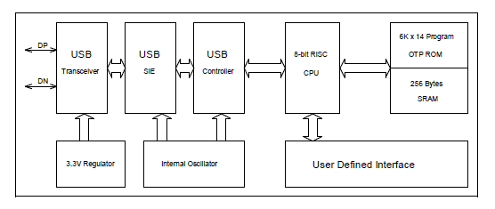
The CX8PU86LV CXUS7719 has program memory size greater 2K works, but the CALL and GOTO instructions only have a 11-bits address range. This 11-bit address range allows a branch within a 2K program memory page size. To allow CALL and GOTO instructions to address the entire 6K program memory address range for CX8PU86LV CXUS7719, there is another two bits to specify the program memory page. The paging bit comes from the ROMBANK[1:0] bits(PUMODE[6:5]). When doing a CALL or GOTO instruction, the user must ensure that page bit ROMBANK[1:0] are programmed so that the desired program memory page is addressed. When one of return instructions is executed, the entire 13-bit PC is POPed from the stack. Therefore, manipulation of the ROMBANK[1:0] is not required for return instructions
二.产品特点
USB Specification Compliance
Support Full-Speed and Low-Speed USB 2.0 specification.
Built-in USB Transceiver.
Built-in 1.5k pull-high resistor.
Support one address and four 8-byte and two 32-byte data endpoints.
Support USB Suspend and Resume function.
One Control IN/OUT endpoints, two INT,BULK endpoints.
8-bit RISC microprocessor
6K x 14 internal program OTP-ROM.
256 bytes internal SRAM.
Optional 12MHz/24MHz internal MCU clock by configuration.
Optional Default/16MHz/12MHz/6MHz/58KHz internal MCU clock by firmware.
One Watch dog Timer ,Timer0,Timer1,and two captures Timers.
System Clock
Internal Oscillator
Internal +/- 4% 24MHz Oscillator
0.25% Accuracy after USB traffic is received.
Internal slow oscillator 58KHz free run clock for suspend mode.
Built-in flexible programming PLL for external Oscillator or crystal
Operating Frequency Range of Oscillator/crystal is 2~48 MHz.
Optional external ceramic resonator or internal clock mode..16-I/O ports
High current drive on any GPIO pin : 25mA/pin current sink.
Each GPIO pin supports high-impedance input, internal pull-ups,
open drains output, or CMOS outputs.
Power Manager and consumption
Power on reset (POR) is 2.0V
Chip can work on greater than 2.2V power.
Low Voltage Detect is 3.8V
Regulator 3.3V output, supply 45mA current.
MCU operating at 24MHz clock
Enable USB operating current is 17mA as Vcc=5V.
Disable USB operating current is 6mA as Vcc=3.3V.
MCU operating at 12MHz clock
Enable USB operating current is 13mA as Vcc=5V.
Disable USB operating current is 4mA as Vcc=3.3V
GPIO supply 1.8V~5V interface.
Support SSC to reduce EMI.
三.应用范围
The CX8PU86LV CXUS7719 is an 8-bit microprocessor embedded device tailored to the
USB application. It includes an 8-bit RISC CPU core, 192~256 byte SRAM, Full Speed and
Low Speed USB Interface and a 6K x 14 internal program OTP-ROM.
四.技术规格书(产品PDF)
需要详细的PDF规格书请扫一扫微信联系我们,还可以获得免费样品以及技术支持!

五.产品封装图

六.电路原理图
七.相关芯片选择指南 更多同类产品......
|
USB |
|||||||||||||||||
|
Product Name |
OTP |
RAM |
I/O |
I/O |
3.3V |
USB |
Stack |
EP0 |
EP1 |
EP2 |
EP3 |
EP4 |
|||||
|
ROM |
Byte |
Voltage |
OUT |
MODE |
|||||||||||||
|
Range |
IN |
OUT |
IN |
OUT |
IN |
OUT |
IN |
OUT |
IN |
OUT |
|||||||
|
4K(OTP) |
192 |
14 |
1.8V~5.5V |
45mA |
INT/BULK |
8 |
64Byte |
64Byte |
64Byte |
64Byte |
64Byte |
64Byte |
64Byte |
64Byte |
NA |
NA |
|
|
6K(OTP) |
192 |
16 |
1.8V~5.5V |
45mA |
INT/BULK |
5 |
8Byte |
8Byte |
8Byte |
NA |
8Byte |
NA |
32Byte |
NA |
NA |
32Byte |
|
|
6K(OTP) |
192 |
16 |
1.8V~5.5V |
45mA |
INT/BULK |
5 |
8Byte |
8Byte |
8Byte |
NA |
8Byte |
||||||
◀ 上一篇:CXUS7717内置USB收发器和3.3V调节器支持USB暂停和恢复功能全速和低速USB 1.1规格PS2兼容接口与USB接口共享通用可编程IO级接口内部时钟发生器8位RISC CPU核心
|
|||||||||||||||||
