7.相关产品
产品概述 返回TOP
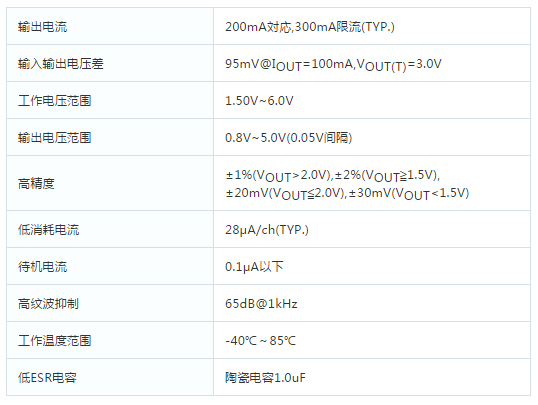
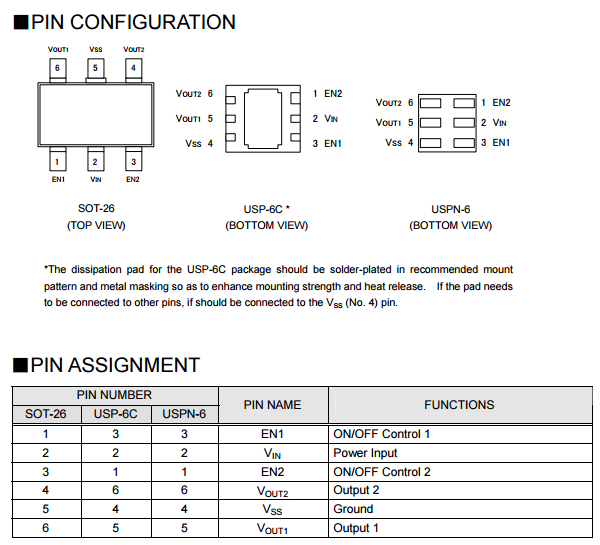
CXLD64211系列是一款高精度,低噪音,高纹波除去率,低压差,采用CMOS工艺的双路LDO电压调整器。由于其在超小型的USP-6C封装内封装了一个低导通阻抗的高速双路LDO,最适合于要求高密度布板的便携式设备。输出电压通过内部激光微调,可以以0.05V的间隔实现0.8V到5.0V之间的任意电压输出。通过EN端,可以实现单独开关各个电压调整器,使其处于关断状态。在此状态下,通过VOUT端和VSS端内置的放电电路,可以瞬间对输出端的电容进行放电。输出端的电容(CL)可以使用低ESR的陶瓷电容。由于其优良的负载响应特性,使其在负载变动的时候也能得到稳定的输出。每个电压调整器完全独立,所以其中一路输出负载发生变动时对另一路输出的影响非常小。The CXLD64211 series is a highly accurate, CMOS Dual LDO voltage regulator. Performance features include low output noise, high ripple rejection rate, and low dropout. Extremely dense power supply circuit can be organized with a 2 channeled high speed voltage regulator in low ON resistance which is built-in to an ultra small USP-6C package. The output voltage for each regulator is set independently by laser trimming and selectable in 0.05V increments within a range of 0.8 to 5.0V. The EN function allows the output of each regulator to be turned off independently. In this state, the electric charge at the output capacitor (CL) will be discharged via the internal auto-discharge switch, and as a result the VOUT pin quickly returns to the VSS level. The output stabilization capacitor (CL) is also compatible with low ESR ceramic capacitors. The high level of output stability is maintained even during frequent load fluctuations, due to the excellent transient response performance. Because regulator 1 and 2 are completely isolated, a cross talk between each channel, which causes a problem during load fluctuations, can be greatly reduced.
产品特点 返回TOP


应用范围 返回TOP
●Smart phones / Mobile phones
●Portable game consoles
●Digital still cameras / camcorders
●Digital audio equipment
●Mobile devices / terminals
技术规格书(产品PDF) 返回TOP
需要详细的PDF规格书请扫一扫微信联系我们,还可以获得免费样品以及技术支持!

产品封装图 返回TOP

电路原理图 返回TOP

|
双路输出电压调整器 |
|||||||||||||
|
产品名称 |
特点 |
封装 |
VIN MIN V |
VIN MAX V |
VOUT MIN V |
VOUT MAX (V) |
IOUT mA |
精度(%) |
输入输 出电压差 (mV) |
消耗 电流 μA |
PSR RdB |
温度范围(℃) |
|
|
Dual LDO |
sot-26w |
1.5 |
6 |
0.8 |
5 |
150 |
±2.0 |
100 |
25 |
70 |
-40~+85 |
||
|
低消耗电流 Dual |
sot-25 |
1.5 |
6 |
0.9 |
5 |
200 |
±2.0 |
320 |
0.8 |
-40~+85 |
|||
|
低消耗电流 Dual |
sot-26 |
1.5 |
6 |
0.9 |
5 |
200 |
±2.0 |
320 |
0.8 |
-40~+85 |
|||
|
高速、双通道 |
sot-26 |
1.5 |
6 |
0.8 |
5 |
200 |
±1.0 |
95 |
28 |
65 |
-40~+85 |
||
|
双路输出 |
sot-26 |
1.5 |
6 |
0.8 |
4 |
200 |
±1.0 |
95 |
10 |
60 |
-40~+85 |
||
|
带ON/OFF功 能双通道输出 |
sot-26 |
1.5 |
6 |
0.8 |
5 |
300 |
±2.0 |
23 |
60 |
-40~+85 |
|||
|
150mA小型高速Dual |
sot26 |
1.6 |
5.5 |
1.2 |
3.6 |
150 |
±1.5 |
130 |
55 |
75 |
-40~+85 |
||
|
带防止突入电流,300mA |
usp-6c |
1.6 |
5.5 |
1.2 |
3.6 |
300 |
±1.0 |
70 |
90 |
75 |
-40~+85 |
||
|
小型300mA,突 入电流防止功能 |
lga-6a01 |
1.6 |
5.5 |
1.2 |
3.6 |
300 |
±1.0 |
64 |
90 |
75 |
-40~+85 |
||