7.相关产品
产品概述 返回TOP
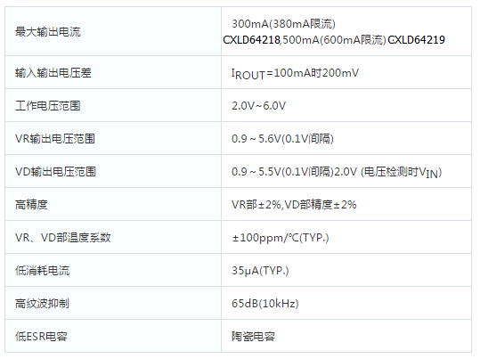
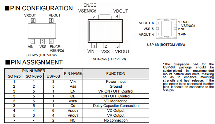
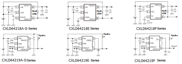
CXLD64218 CXLD64219是内置电压检测器的具有高精度,低噪声,低电压差的正电压输出电压调整器。该系列采用CMOS工艺技术,具有高电源抑制比和低压差的特点。内部由基准电压电路,误差放大电路,限流电路,相位补偿电路以及一个驱动三极管组成。该系列可以使用低ESR的陶瓷电容,使得输出更稳定,由于良好的瞬态响应特性,在负载条件发生变化条件下也仍保持一个稳定的输出。内置的限流Foldback电路同样也具有短路保护功能。CXLD64218 CXLD64219的A到C系列:通过控制使能端子EN,可以使得内置的电压调整器处于待机状态。CXLD64218 CXLD64219的D,F系列(客户定制):通过控制CE端子的电平可以使得整个芯片处于待机状态。在待机状态下芯片的功耗会大大降低。CXLD64218 CXLD64219的A和B系列具有toggle功能。CXLD64218 CXLD64219B(客户定制)的电压检测器监测到电压时可以关断电压调整器的输出。CXLD64218 CXLD64219E定制系列,通过VSEN端子来检测其他电源电压。通过外部连接的电容可以调节电压检测器的延迟时间长短。The CXLD64218 CXLD64219 series are highly precise, low noise, high current, positive voltage low dropout regulators with built-in voltage detector. They are fabricated using CMOS process. Performance features of the series includes high ripple rejection and low dropout voltage, and the series features a voltage reference, an error amplifier, a current limiter and a phase compensation circuit plus a driver transistor. Detect voltage is selectable in 100mV increments within the range of 0.9V to 5.6V and the LDO output voltage is selectable within a range of 0.9V to 5.6V (CXLD64218 CXLD64219) 0.9V to 5.1V (CXLD64219), also in 100mV increments. The series is also compatible with low ESR ceramic capacitors which give added output stability. This stability can be maintained even during load fluctuations due to the excellent transient response of the series. The current limiter's foldback circuit also operates as a short circuit protection for the output current limiter and the output pin. The series provides options to the user to select from a variety of circuit features, such as detector monitoring, detector output logic, CE and EN pin input logic, internal pull-up / down resistance, and power ready. The IC's internal regulator circuit can be placed in stand-by mode via the EN function (CXLD64218/CXLD64219A to C series). The whole IC can be put in to stand-by mode via the CE function with the CXLD64218 /CXLD64219D series (semi-custom). In the stand-by mode, power consumption is greatly reduced. The CXLD64218/CXLD64219A and B series features the toggle operation function. The regulator output can be OFF when the CXLD64218 /CXLD64219B series detects voltage (semi-custom). The CXLD64218 /CXLD64219E series can monitor another power source by using the VSEN pin (semi-custom). The XCXLD64218 CXLD6421904F series can delay the detector output: the delay time can be controlled by the use of an external capacitor (semi-custom).
产品特点 返回TOP

应用范围 返回TOP
●CD-ROM, CD-R / RW drive
●DVD drive
●HDD drive
●Cameras, Video recorders
●Portable AV equipment
●Battery powered equipment
技术规格书(产品PDF) 返回TOP
需要详细的PDF规格书请扫一扫微信联系我们,还可以获得免费样品以及技术支持!

产品封装图 返回TOP

电路原理图 返回TOP

|
电压调整器带复位端子 |
||||||||||||
|
产品名称 |
特点 |
封装 |
VIN MIN |
VIN MAX |
VOUT MIN |
VOUT MAX |
IOUT mA |
精度 (%) |
输入输 出电压 差(mV) |
消耗 电流 μA |
PSRR dB |
温度范围 (℃) |
|
(V) |
(V) |
(V) |
(V) |
|||||||||
|
大电流VD付 |
SOT25 SOT89 USP6B |
1.5 |
6 |
0.8 |
5 |
700 |
±2.0 |
50 |
35 |
60 |
-40~+85 |
|
|
高速低压差电压调整器 |
SOT25 SOT89 USP6B |
2 |
6 |
0.9 |
5.1 |
500 |
±2.0 |
200 |
35 |
65 |
-40~+85 |
|
|
高速低压差电压调整器 |
SOT25 SOT89 USP6B |
2 |
6 |
0.9 |
5.1 |
500 |
±2.0 |
200 |
35 |
65 |
-40~+85 |
|
|
高速LDO VD付 |
SOT25 SOT89 USP6B |
2 |
6 |
0.9 |
5.1 |
500 |
±2.0 |
200 |
90 |
65 |
-40~+85 |
|
|
28V耐圧 |
SOT25 SOT89 USP6C |
2 |
28 |
2 |
18 |
150 |
±1.0 |
1100 |
8 |
-40~+85 |
||
|
10V输入带电压检测器 |
SOT25 SOT89 USP6B |
2 |
10 |
0.9 |
5.5 |
500 |
±2.0 |
200 |
35 |
65 |
-40~+85 |
|
|
10V输入带电压检测器 |
SOT25 SOT89 USP6B |
2 |
10 |
0.9 |
5.5 |
500 |
±2.0 |
200 |
35 |
65 |
-40~+85 |
|